In-Circuit Testing (ICT) is a widely used method in electronics manufacturing for the detection of faults and defects in printed circuit boards (PCBs). It involves testing individual components and connections on a PCB to ensure proper functionality and adherence to design specifications. This is also the most convenient way to load software into the product. ICT can detect PCB assembly faults and anomalies in functions before the final assembly stages.
One of the primary benefits of using in-circuit testing is its ability to detect defects early in the manufacturing process, saving time and cost associated with diagnosing and rectifying faults later on.
ICT offers several advantages:
- Comprehensive Fault Detection: ICT can identify a wide range of electrical faults, including shorts, opens, and components with incorrect values, allowing for thorough testing of the circuitry.
- High Test Coverage: With its ability to test individual components and connections, ICT provides high test coverage, ensuring that most of the critical circuitry is examined during the testing process.
- Fast Testing: ICT can perform tests quickly, enabling efficient production throughout and reducing the time required for testing each PCB. ICT catches around 98% of faults on the board and it takes just a few minutes per PCB.
- Cost-Effective: By catching faults early, ICT helps prevent defective products from progressing further in the manufacturing process, reducing scrap, rework, and customer returns.
Considering ICT, remember that it can be expensive and time-consuming in some cases. Some of the examples include having a complex PCB design, such as those with a high component density or multiple layers. Testing all the connections and components in such a design can be challenging and may require specialized fixtures and equipment, increasing the overall cost. Manufacturing low volumes of PCBs, and the cost of setting up and programming the ICT system could also outweigh the benefits.
In the context of the Internet of Things (IoT), ICT plays a crucial role in ensuring the quality and reliability of IoT devices. IoT devices typically consist of complex PCBs with numerous components, making ICT an effective method to verify their functionality. For example, in manufacturing IoT sensors, ICT can detect faults such as misaligned sensor connections or faulty sensor components. This ensures that the sensors operate correctly and provide accurate data for IoT applications like environmental monitoring, industrial automation, and smart homes.
Examples of how we have developed ICT solutions
Valnes
Valnes was looking for a partner who could design and develop a next-generation smart lock device that could manage the access of doors remotely via the internet, using any computer or smart device.
Valnes Digital Access Control PCBs are tested with the ICT on-site at EMS. Since the boards undergo a coating procedure at the end of the manufacturing process, it is necessary to test the units before rework becomes impractical. The ICT has roughly a hundred test points – all required to program, test and provision the DUT (Device Under Testing).
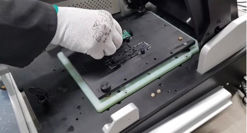
Testing in Incap Estonia.
SportScientia
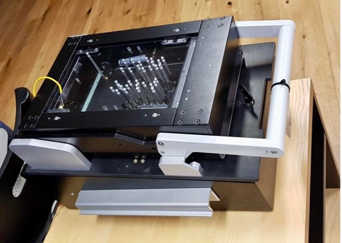
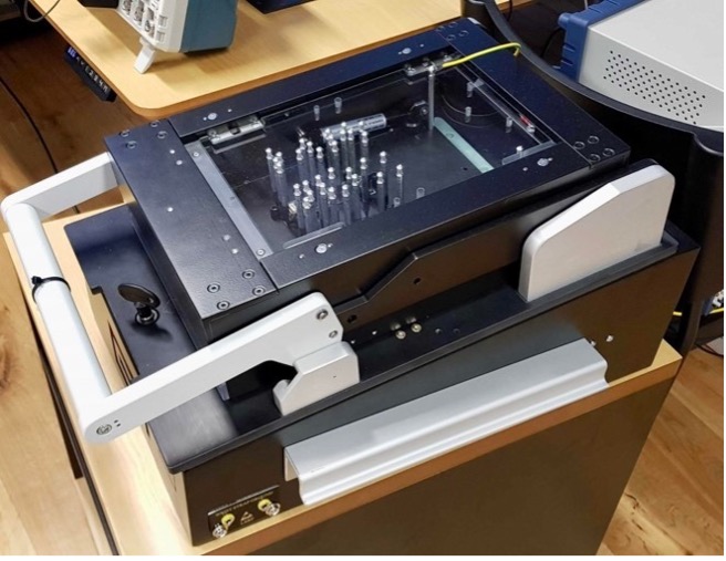
Krakul has been working with SportScientia to develop a precision instrument to capture high-quality foot-to-surface data for physiotherapists, medical and sports practitioners. The complexity of producing such technology led to great challenges when considering all the different stages of the production process. Because of the intertwined processes of PCB manufacturing and mechanical assembling, the testing was, along with the customer, decided to be implemented in three phases.
- Initial hardware functionality test and flashing: The PCB is placed on the tester and the first phase is activated. The MCU is programmed, and the generated serial numbers are automatically uploaded to a server holding the data of all the manufacturing runs. Initial connection tests are run to ensure the MCU can see and communicate with all the peripherals.
- Hardware functionality test after potting: Because of the nature of potting, it is important to know if the hardware still functions before the device is completely assembled. This testing happens after two different PCBs have been connected and potted together. In this stage, both the functionality of the second PCB and the mechanical production quality are validated. The QR code of the second PCB is scanned by the operator and can be uploaded to the server to join the two different PCBs together in the database, ultimately providing a comprehensive history of each sub-assembly of the final product.
- Validating functionalities: The third phase is executed after the device has been fully assembled. This will validate the device's functionalities after the final assembly processes (in this example, the last sensors soldered to the device after potting and before adding glue to hold everything together).
These tests are run in stages because of the complexity of the manufacturing process and have been developed and discussed with the customer during the development of the device itself. The main purpose of chopping the process up into different stages is to reduce waste and by that, also the cost. A faulty PCB will never make it past the first stage of the process – thereby no further resources will be spent on it. In addition, it also allows the product owner and our developers to get the statistical data about where the manufacturing process most often goes wrong – and work on improvements to reduce errors or find better solutions for the manufacturer.
Ampler
Ampler is a leading e-bike producer, gaining prominence in the industry for its cutting-edge electric bicycle designs. Over the years, Krakul has been fortunate to collaborate closely with Ampler, providing them with comprehensive hardware and firmware development solutions. As technology partners, we have played a pivotal role in enhancing the performance, functionality, and connectivity of Ampler's e-bikes.
Tight cooperation between product design, test design team, and product owner was needed for optimal and successful tester deployment.
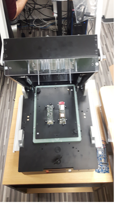
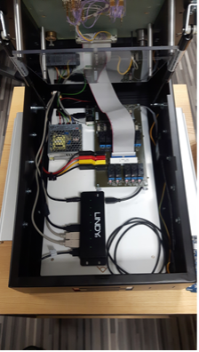
The tester project had three broad steps.
- Tester specification phase: In this phase, we agreed on what will be tested and how. This usually depends on the cost of failed units, intended production volumes, budget for the tester EMS preferences, and unit serializing requirements. With this process, we will create the test specification with details about interfaces, and test equipment, and create a list of test points.
- Tester development: We source and assemble necessary equipment, and write the software, operating guide, and maintenance instructions. Ease of maintenance is prioritized so a technician could troubleshoot the tester and fix most of the issues.
- Tester deployment: If needed, a team from Krakul will accompany the tester at its deployment on the EMS site. We will perform the initial setup, instruct the operators in the first test cycles, and ensure the test step fits well into the production flow.
In Conclusion
Krakul has partnered with electronics manufacturing services to ensure that production costs stay low, and testing is fast and effective. We can perform a wide variety of tests on different products to maintain quality control and cut down on simple software failures, and errors with PCBs and firmware. Designing PCBs and ICT in parallel makes it easier to scale production volumes and put the product into series production.
If you need advice with in-circuit testing or looking for an IoT development partner for your business, our experienced engineers can help you!
Krakul has been developing custom IoT devices for customers globally since 2013.
Book a quick intro call with us!